| CPC H10B 12/34 (2023.02) [H10B 12/053 (2023.02); H10B 12/482 (2023.02); H10B 12/485 (2023.02)] | 15 Claims |
|
1. A method of forming a semiconductor memory device, comprising;
providing a substrate;
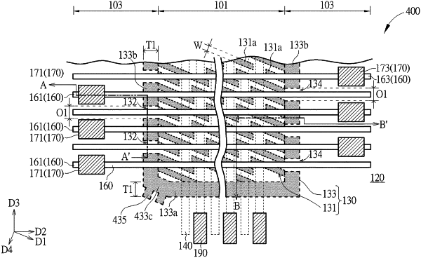
forming an active structure in the substrate, the active structure comprising:
a first active region comprising a plurality of active region units parallel with each other and extending along a first direction; and
a second active region disposed at an outer side of the first active region, the second active region comprising a first edge extending along a second direction and a second edge extending along a third direction, and the first edge and the second edge directly connected to a portion of the active region units, wherein the second active region comprises a plurality of first openings, and the first openings are disposed on the second edge; and
forming a shallow trench isolation in the substrate, the shallow trench isolation surrounding the active structure.
|