| CPC H05K 3/4688 (2013.01) [H05K 1/0251 (2013.01); H05K 1/116 (2013.01); H05K 3/0094 (2013.01); H05K 2201/0959 (2013.01); H05K 2201/09518 (2013.01)] | 10 Claims |
|
1. A multilayer circuit board, comprising:
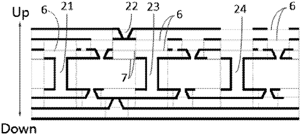
a plurality of metal layers, a blind via and a buried via, wherein the multilayer circuit board is configured to transmit signals between different ones of the metal layers through a metal line of the corresponding metal layers and the blind via or the buried via, wherein the blind via includes a pad disposed on a non-opening side of the blind via, and the buried via includes a pad disposed on each of an upper orifice and a lower orifice thereof, wherein
an upper or lower metal layer on the non-opening side of the blind via that is adjacent to a metal layer including the blind via has a first hole which is located in a position corresponding to the pad on the non-opening side of the blind via and in a depth direction of the blind via, a projection of the first hole completely covers a projection of the pad on the non-opening side of the blind via on a surface perpendicular to the depth direction of the blind via, wherein the first hole has a diameter that is equal to or larger than a diameter of the pad on the non-opening side of the blind via;
an upper and/or lower metal layer that is adjacent to a metal layer including the buried via has a second hole which is located in a position corresponding to the pad of the upper orifice and/or the lower orifice of the buried via and in a depth direction of the buried via, a projection of the second hole completely covers a projection of the pad on the upper orifice or lower orifice of the buried via on a surface perpendicular to the depth direction of the buried via, wherein the second hole has a diameter that is equal to or larger than a diameter of the pad on the upper orifice and/or the lower orifice of the buried via.
|