|
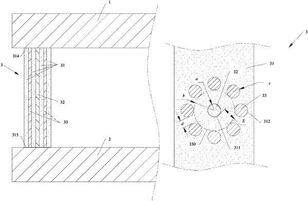
1. An electronic device, comprising: a housing; a display screen fastened to the housing and configured to display an image; and a circuit board assembly accommodated in the housing, the circuit board assembly comprising: a first circuit board having a first component disposed thereon; a second circuit board having a second component disposed thereon, wherein the second circuit board is stacked with the first circuit board, wherein the first circuit board includes a first ground and/or the second circuit board includes a second ground; and a connection plate disposed between the first circuit board and the second circuit board, the connection plate including a plate body, wherein a first end of the plate body is connected to the first circuit board, and a second end of the plate body is connected to the second circuit board; the connection plate including: a signal transmission hole extending from the first end of the plate body to the second end of the plate body, a signal transmission part disposed in the signal transmission hole configured to transmit a first signal between the first circuit board and the second circuit board, at least one ground hole disposed at a spacing to the signal transmission hole and extending from the first end of the plate body to the second end of the plate body, and a ground part disposed in the at least one ground hole configured to connect to the first ground and/or the second ground, the circuit board assembly further comprises: a first signal transmission pad and at least one first ground pad, disposed on a side that is of the first circuit board and that faces the connection plate; a second signal transmission pad and at least one second ground pad, disposed on a side of the second circuit board that faces the connection plate; two ends of the signal transmission part are respectively welded to the first signal transmission pad and the second signal transmission pad, and two ends of the grounding part are respectively welded to the first grounding pad and the second grounding pad.
|