|
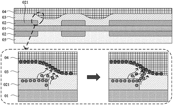
1. A circuit board, comprising: at least one circuit board unit sequentially stacked in a thickness direction of the circuit board, the circuit board unit including a substrate layer and two conductive layers respectively disposed on two opposite sides of the substrate layer in a thickness direction of the substrate layer, and each of the conductive layers including a plurality of signal lines; an insulating layer located on a side of an outermost conductive layer away from the substrate layer; an electromagnetic shielding layer located on a side of the insulating layer away from the substrate layer; and a barrier layer located between the electromagnetic shielding layer and the outermost conductive layer; the barrier layer at least covering a plurality of signals lines in the outermost conductive layer, wherein the outermost conductive layer has a signal line region, and the plurality of signal lines in the outermost conductive layer are located in the signal line region; a contour line of an orthogonal projection of the signal line region of the outermost conductive layer on the substrate layer is within a range of a contour line of an orthogonal projection of the barrier layer on the substrate laver.
|