US 11,706,525 B2
Image sensor including light shielding layer and patterned dielectric layer
Yun-Wei Cheng, Taipei (TW); Chun-Hao Chou, Tainan (TW); Hsin-Chi Chen, Tainan (TW); Kuo-Cheng Lee, Tainan (TW); and Hsun-Ying Huang, Tainan (TW)
Assigned to Taiwan Semiconductor Manufacturing Company, Ltd., Hsinchu (TW)
Filed by Taiwan Semiconductor Manufacturing Company, Ltd., Hsinchu (TW)
Filed on Oct. 4, 2021, as Appl. No. 17/493,752.
Application 17/493,752 is a continuation of application No. 16/699,752, filed on Dec. 2, 2019, granted, now 11,140,309.
Application 16/699,752 is a continuation of application No. 15/866,481, filed on Jan. 10, 2018, granted, now 10,498,947, issued on Dec. 3, 2019.
Claims priority of provisional application 62/578,531, filed on Oct. 30, 2017.
Prior Publication US 2022/0030158 A1, Jan. 27, 2022
Int. Cl. H04N 5/232 (2006.01); H04N 23/67 (2023.01); H01L 27/146 (2006.01); H04N 23/10 (2023.01); H04N 25/133 (2023.01); H04N 25/13 (2023.01); H04N 25/702 (2023.01); H04N 25/704 (2023.01); H04N 5/369 (2011.01)
CPC H04N 23/67 (2023.01) [H01L 27/1463 (2013.01); H01L 27/14603 (2013.01); H01L 27/14621 (2013.01); H01L 27/14627 (2013.01); H01L 27/14689 (2013.01); H04N 23/10 (2023.01); H04N 25/133 (2023.01); H04N 25/134 (2023.01); H04N 25/702 (2023.01); H04N 25/704 (2023.01)] 20 Claims
OG exemplary drawing
 
1. An image sensor, comprising:
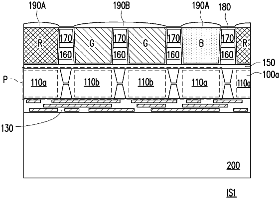
a semiconductor substrate comprising sensing pixels, each sensing pixel comprising a first sub-pixel, a second sub-pixel and a pair of third sub-pixels with phase detection function;
color filters disposed over the sensing pixels;
lenses covering the color filters; and
a grid structure disposed between the color filters and located over the isolation structures, wherein the grid structure comprises:
a shielding grid layer; and
a dielectric grid layer covering the shielding grid layer, wherein the color filters are space apart from each other by the grid structure.