| CPC H04N 23/57 (2023.01) [G06F 1/163 (2013.01); G09F 9/30 (2013.01); H01L 27/14 (2013.01); H01L 27/144 (2013.01); H01L 27/146 (2013.01); H01L 27/15 (2013.01); H01L 27/32 (2013.01); H01L 31/02019 (2013.01); H01L 31/02164 (2013.01); H01L 31/10 (2013.01); H01L 31/147 (2013.01); H01L 51/50 (2013.01); H04N 23/56 (2023.01); H04N 25/70 (2023.01); H05B 33/02 (2013.01); H05B 33/12 (2013.01); H05B 33/14 (2013.01)] | 36 Claims |
|
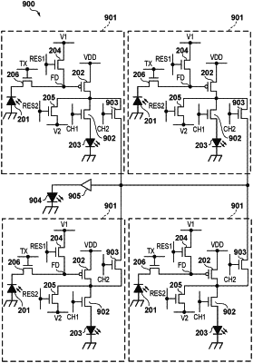
1. An apparatus comprising:
a first portion including a first semiconductor layer, a photoelectric conversion element, a first connecting portion, a first conductive pattern electrically connected to the first connecting portion, and a first insulator; and
a second portion including a second semiconductor layer, a light-emitting element, a second connecting portion, a second conductive pattern electrically connected to the second connecting portion, and a second insulator,
wherein the first portion and the second portion are stacked on each other, and
wherein the first connecting portion and the second connecting portion are directly connected to each other or are connected via a micro bump.
|