| CPC H03K 3/037 (2013.01) [G11C 17/16 (2013.01); G11C 17/18 (2013.01); H03K 19/20 (2013.01)] | 10 Claims |
|
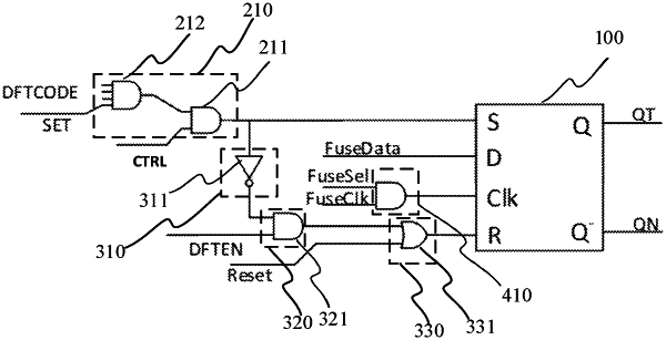
1. A latch circuit, characterized in comprising:
a latch module, for latching data input by a data module;
a set control module, for controlling the latch module to output a high-level signal, input signals of the set control module including a control signal and a set signal;
a reset control module, for controlling the latch module to output a low-level signal, input signals of the reset control module including an output signal of the set control module, a self-test enable signal and a reset signal; and
a clock module, for providing a readout clock signal to the latch module;
wherein the self-test enable signal decides whether the latch circuit is in a self test mode or a normal operation mode.
|