| CPC H03K 3/012 (2013.01) [G11C 7/1051 (2013.01); G11C 7/1078 (2013.01); H03K 3/356113 (2013.01); H03K 19/0185 (2013.01); H03K 19/017509 (2013.01)] | 18 Claims |
|
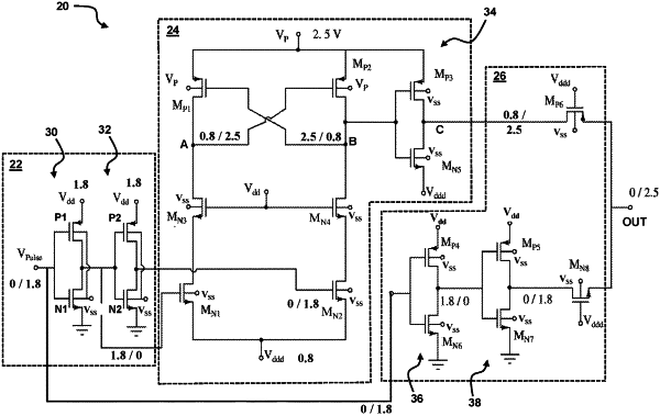
1. A level shifter, comprising:
first and second NMOS transistors each including a gate, drain, and source, wherein the sources of the first and second NMOS transistors are coupled to a first voltage, wherein the gate of the first NMOS transistor is connected to an inverse of an input signal that varies between a second voltage and a third voltage, and wherein the gate of the second NMOS transistor receives a buffer of the input signal;
a breakdown protection circuit including third and fourth NMOS transistors each including a gate, drain, and source, wherein the gates of the third and fourth NMOS transistors are connected to the third voltage, the drain of the first NMOS transistor is connected to the source of the third NMOS transistor, and the drain of the second NMOS transistor is connected to the source of the fourth NMOS transistor; and
a pull-up circuit supplied by a fourth voltage and connected to the drains of the third and fourth NMOS transistors, the pull-up circuit including:
a first PMOS transistor including a gate, drain, and source; and
a second PMOS transistor including a gate, drain, and source,
wherein the drain of the third NMOS transistor is connected to the drain of the first PMOS transistor and the gate of the second PMOS transistor, wherein the drain of the fourth NMOS transistor is connected to the drain of the second PMOS transistor and the gate of the first PMOS transistor, and wherein the sources of the first and second PMOS transistors are coupled to the fourth voltage, and
wherein the first voltage is greater than the second voltage, the third voltage is greater than the first voltage, and the fourth voltage is greater than the third voltage.
|