| CPC H01L 33/62 (2013.01) [H01L 25/0753 (2013.01); H01L 33/56 (2013.01); H01L 2924/15151 (2013.01); H01L 2924/3641 (2013.01)] | 20 Claims |
|
1. A display apparatus comprising:
a substrate having a display area and a peripheral area surrounding the display area;
a first initialization voltage line on the substrate;
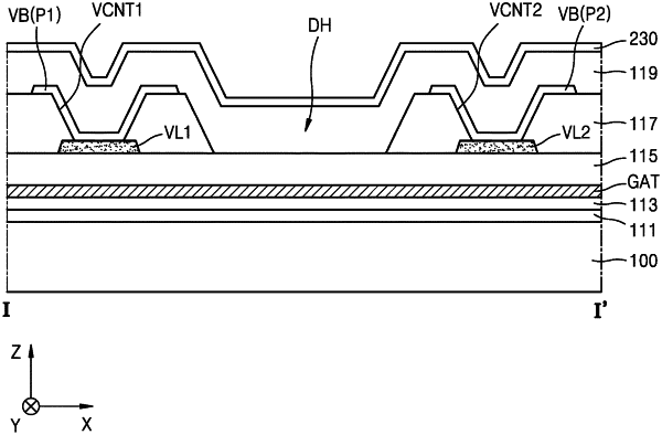
an organic film layer on the first initialization voltage line and having a first contact hole exposing at least a portion of the first initialization voltage line;
a bridge wiring on the organic film layer corresponding to the peripheral area, and in contact with the first initialization voltage line through the first contact hole;
an insulating layer on the organic film layer and comprising an organic insulating material; and
a plurality of pixels on the display area and each receiving an initialization voltage,
wherein the organic film layer corresponding to the peripheral area has a groove or dummy hole, the groove or the dummy hole being adjacent to the first contact hole,
wherein the insulating layer contacts the bridge wiring and walls of the groove or the dummy hole.
|