| CPC H01L 33/60 (2013.01) [H01L 33/38 (2013.01); H01L 33/46 (2013.01); H01L 33/54 (2013.01); H01L 33/56 (2013.01)] | 19 Claims |
|
1. A light-emitting device, comprising:
a substrate, comprising a sidewall, a first top surface and a second top surface, wherein the second top surface is closer to the sidewall of the substrate than the first top surface to the sidewall of the substrate;
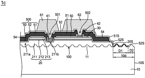
a semiconductor stack formed on the substrate, the semiconductor stack comprising a first semiconductor layer, an active layer and a second semiconductor layer, wherein the first semiconductor layer comprises a first mesa continuously surrounding a periphery of the semiconductor stack;
a dicing street surrounding the semiconductor stack and exposing the first top surface and the second top surface of the substrate;
a protective layer covering the semiconductor stack;
a reflective layer comprising a Distributed Bragg Reflector structure, covering the protective layer and the first mesa, wherein the reflective layer does not contact the first mesa; and
a cap layer, covering the reflective layer,
wherein the first top surface and the second top surface of the substrate are not covered by the reflective layer, and
wherein the cap layer does not contact the substrate.
|