| CPC H01L 33/38 (2013.01) [H01L 27/156 (2013.01); H01L 33/62 (2013.01); H01L 27/1251 (2013.01); H01L 2933/0016 (2013.01); H01L 2933/0066 (2013.01)] | 8 Claims |
|
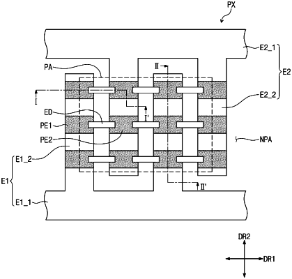
1. A manufacturing method of a display device, the method comprising:
providing a first conductive material on a substrate;
providing a second conductive material on the first conductive material;
providing a first photoresist pattern comprising a first portion on the second conductive material and a plurality of second portions spaced apart from each other and disposed on the first portion;
removing portions of the first and second conductive materials that are exposed by the first photoresist pattern to form a first electrode and a second electrode defined by remaining portions of the first conductive material;
removing the first photoresist pattern from an upper portion of the first photoresist pattern by a thickness of the first portion to form a second photoresist pattern;
removing portions of the second conductive material that are exposed by the second photoresist pattern to form a plurality of first protruding electrodes and a plurality of second protruding electrodes; and
electrically connecting a plurality of light emitting elements to the plurality of first protruding electrodes and the plurality of second protruding electrodes.
|