| CPC H01L 29/7881 (2013.01) [H01L 21/26513 (2013.01); H01L 21/76224 (2013.01); H01L 29/0653 (2013.01); H01L 29/0847 (2013.01); H01L 29/40114 (2019.08); H01L 29/42328 (2013.01); H01L 29/66825 (2013.01)] | 10 Claims |
|
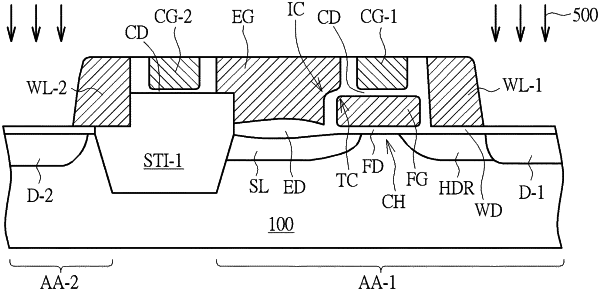
1. A method of forming a semiconductor memory device, comprising:
providing a substrate comprising a first active area and a second active area in proximity to the first active area;
forming a trench isolation region between the first active area and the second active area;
forming a floating gate on the first active area;
forming a first control gate on the floating gate and a second control gate on the trench isolation region;
performing a first ion implantation process to form a source line region in the first active area and adjacent to the trench isolation region, and a heavily doped region in the first active area and spaced apart from the source line region;
forming an erase gate on the source line region;
forming a first word line adjacent to the floating gate and the first control gate; and
forming a second word line adjacent to the second control gate.
|