| CPC H01L 29/78633 (2013.01) [G02F 1/1368 (2013.01); H01L 27/1225 (2013.01); H01L 29/7869 (2013.01); H01L 29/78693 (2013.01); H10K 59/123 (2023.02); H10K 59/126 (2023.02); H10K 2102/311 (2023.02)] | 41 Claims |

|
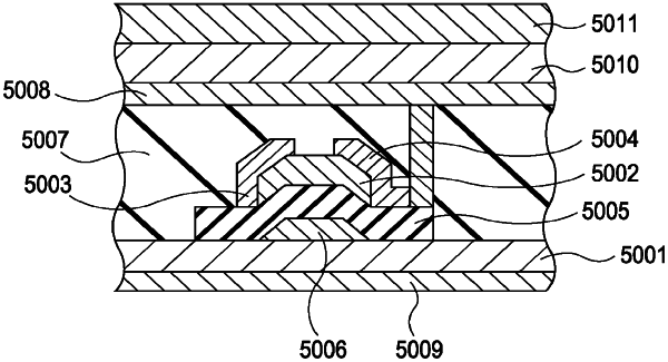
1. A display, comprising:
a field-effect transistor;
an interlayer-insulating film covering the field-effect transistor;
a light-emitting device emitting light over the interlayer-insulating film; and
a light-shielding member containing a metal;
the field-effect transistor comprising an active layer containing a transparent oxide, a gate electrode containing a metal, a gate-insulating film between the active layer and the gate electrode, a first electrode in contact with the active layer, and a second electrode in contact with the active layer; and
the light-emitting device comprising a third electrode, a fourth electrode between the third electrode and the interlayer-insulating film, and a light-emitting layer between the third electrode and the fourth electrode, wherein
the gate electrode and the active layer are disposed between the fourth electrode and the light-shielding member in a first direction perpendicular to a surface of the light-shielding member, and
the gate electrode has both ends in a second direction perpendicular to the first direction, and both ends of the gate electrode are disposed between the fourth electrode and the light-shielding member in the first direction.
|