| CPC H01L 29/7851 (2013.01) [H01L 21/823431 (2013.01); H01L 27/0886 (2013.01); H01L 29/0673 (2013.01); H01L 29/1054 (2013.01); H01L 29/42392 (2013.01); H01L 29/78696 (2013.01)] | 19 Claims |
|
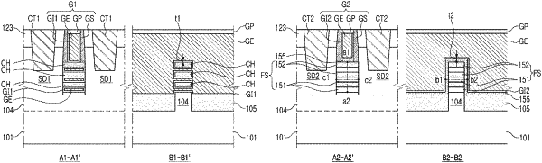
1. A semiconductor device comprising:
a substrate;
a first transistor on a first region of the substrate, the first transistor including:
a plurality of channel layers spaced apart from each other in a first direction perpendicular to an upper surface of the substrate;
a first gate electrode surrounding the plurality of channel layers;
a first gate insulating film between the plurality of channel layers and the first gate electrode; and
first source/drain regions on opposite side surfaces, respectively, of the plurality of channel layers, and electrically connected to each of the plurality of channel layers;
a second transistor on a second region of the substrate, the second transistor including:
a fin structure having a plurality of first semiconductor patterns and a plurality of second semiconductor patterns, alternately stacked;
a second gate electrode on an upper surface and opposite side surfaces of the fin structure;
a second gate insulating film between the fin structure and the second gate electrode; and
second source/drain regions on the side surfaces, respectively, of the fin structure,
wherein each of the plurality of first semiconductor patterns has a first germanium (Ge) content gradient that increases toward a first center thereof in the first direction, and a first Ge content in the first center of each of the first semiconductor patterns is in a first range of 25% to 35%.
|