| CPC H01L 29/7843 (2013.01) [H01L 21/0217 (2013.01); H01L 21/76224 (2013.01); H01L 21/823412 (2013.01); H01L 21/823431 (2013.01); H01L 21/823437 (2013.01); H01L 21/823481 (2013.01); H01L 27/0924 (2013.01); H01L 29/0673 (2013.01); H01L 29/0847 (2013.01); H01L 29/1033 (2013.01); H01L 29/42392 (2013.01); H01L 29/66545 (2013.01); H01L 29/66553 (2013.01); H01L 29/66795 (2013.01); H01L 29/785 (2013.01); H01L 21/0262 (2013.01); H01L 21/02532 (2013.01); H01L 21/26513 (2013.01); H01L 21/3065 (2013.01); H01L 21/3081 (2013.01); H01L 21/31116 (2013.01)] | 20 Claims |
|
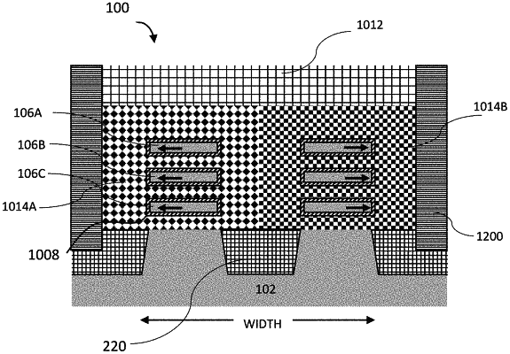
1. A semiconductor device comprising:
a nanosheet stack formed on a substrate, the nanosheet stack comprising nanosheet channels;
source and drain regions formed on the substrate;
a gate around the nanosheet stack;
a spacer formed on a sidewall of the gate;
an inter-layer dielectric formed adjacent to the spacer; and
a trench formed in a portion of the gate, the spacer, and the inter-level dielectric and extending toward the substrate, wherein the trench is filled with a strained material.
|