| CPC H01L 29/78391 (2014.09) [H01L 29/24 (2013.01); H01L 29/516 (2013.01); H01L 29/6684 (2013.01); H01L 29/66969 (2013.01)] | 20 Claims |
|
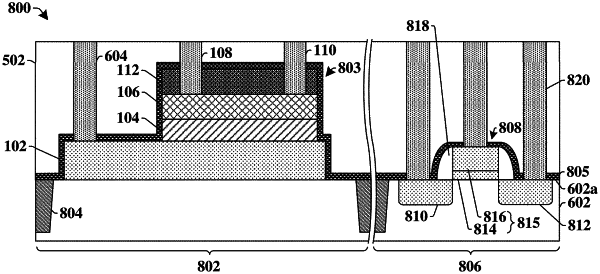
1. A method of forming a FeFET device, comprising:
forming a FeFET stack comprising a polarization enhancement structure disposed on an oxide semiconductor that is separated from a gate structure by a ferroelectric structure, wherein the polarization enhancement structure comprises a semiconductor, and wherein the oxide semiconductor has a different semiconductor type than the polarization enhancement structure;
forming a dielectric layer on the polarization enhancement structure;
performing a first patterning process to form a source opening and a drain opening that extend through the polarization enhancement structure to expose the oxide semiconductor; and
forming a conductive material within the source opening and the drain opening.
|