| CPC H01L 29/7786 (2013.01) [H01L 29/401 (2013.01); H01L 29/4236 (2013.01); H01L 29/42356 (2013.01); H01L 29/42364 (2013.01); H01L 29/66462 (2013.01)] | 29 Claims |
|
1. A metal-insulator-semiconductor device, comprising:
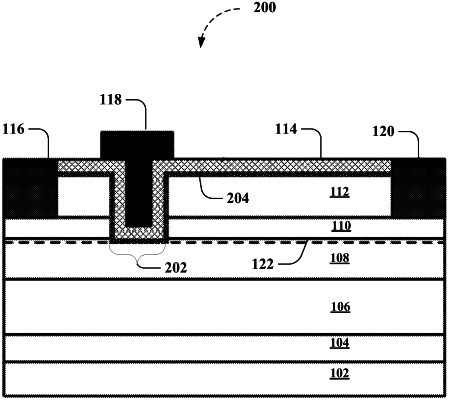
a recessed gate structure that is recessed into a portion of a barrier layer and a channel layer of the metal-insulator-semiconductor device;
an interface protection layer adjacent to the recessed gate structure, wherein the interface protection layer is located at a gate foot area of the recessed gate structure; and
a gate dielectric layer disposed on the interface protection layer, wherein the gate dielectric layer is located between a gate electrode and the channel layer, wherein the gate dielectric layer comprises a low-pressure chemical vapor deposited silicon nitride formation that was deposited at or above about 780 degrees Celsius, wherein the interface protection layer is located between the gate dielectric layer and the channel layer and comprises an oxidized portion of the channel layer at the gate foot area of the recessed gate that was oxidized at or below about 300 degrees Celsius, wherein the interface protection layer comprises a uniform surface morphology at an interface between the channel layer and the gate dielectric layer, and wherein the interface protection layer is adapted to protect the channel layer from surface decomposition associated with gate dielectric deposition.
|