| CPC H01L 29/66795 (2013.01) [H01L 21/0262 (2013.01); H01L 21/02488 (2013.01); H01L 21/02513 (2013.01); H01L 21/02532 (2013.01); H01L 21/02592 (2013.01); H01L 21/02598 (2013.01); H01L 21/02639 (2013.01); H01L 21/02661 (2013.01); H01L 21/02675 (2013.01); H01L 21/31116 (2013.01); H01L 29/0847 (2013.01); H01L 29/66545 (2013.01); H01L 29/785 (2013.01); H01L 21/02576 (2013.01); H01L 21/02579 (2013.01); H01L 21/30604 (2013.01)] | 20 Claims |
|
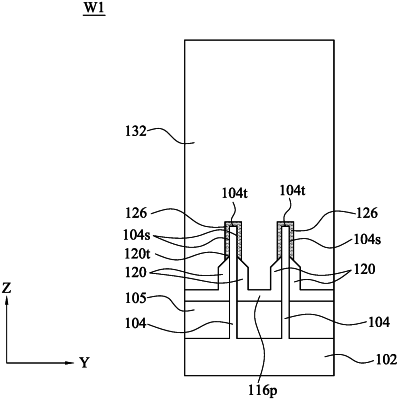
1. A method, comprising:
forming a semiconductor fin extending from a substrate;
forming a shallow trench isolation (STI) region around a lower portion of the semiconductor fin;
performing a deposition process to form a silicon layer having a crystalline silicon portion over the semiconductor fin and an amorphous silicon portion over the STI region;
performing an anneal process to crystallize the amorphous silicon portion into a polysilicon portion; and
selectively etching the polysilicon portion, while leaving the crystalline silicon portion over the semiconductor fin.
|