| CPC H01L 29/66545 (2013.01) [H01L 29/0673 (2013.01); H01L 29/0847 (2013.01); H01L 29/42392 (2013.01); H01L 29/78696 (2013.01)] | 15 Claims |
|
1. A method for forming a semiconductor device, the method comprising:
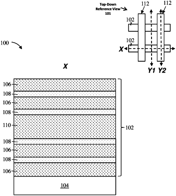
forming a nanosheet stack over a substrate, the nanosheet stack comprising alternating first sacrificial layers and second sacrificial layers, wherein one layer of the first sacrificial layers comprises a greater thickness than the remaining first sacrificial layers;
removing the first sacrificial layers;
forming semiconductor layers on surfaces of the second sacrificial layers, wherein the semiconductor layers comprise a first set and a second set of semiconductor layers;
removing the second sacrificial layers; and
forming an isolation dielectric between the first set and the second set of semiconductor layers.
|