US 11,705,496 B2
Charge-trapping layer with optimized number of charge-trapping sites for fast program and erase of a memory cell in a 3-dimensional NOR memory string array
Wu-Yi Henry Chien, San Jose, CA (US); Scott Brad Herner, Portland, OR (US); and Eli Harari, Saratoga, CA (US)
Assigned to SUNRISE MEMORY CORPORATION, San Jose, CA (US)
Filed by SUNRISE MEMORY CORPORATION, San Jose, CA (US)
Filed on Apr. 5, 2021, as Appl. No. 17/222,082.
Claims priority of provisional application 63/007,244, filed on Apr. 8, 2020.
Prior Publication US 2021/0320182 A1, Oct. 14, 2021
Int. Cl. H01L 29/423 (2006.01); H01L 29/792 (2006.01); H01L 29/786 (2006.01); H10B 43/30 (2023.01)
CPC H01L 29/42348 (2013.01) [H01L 29/78642 (2013.01); H01L 29/78672 (2013.01); H01L 29/7926 (2013.01); H10B 43/30 (2023.02)] 8 Claims
OG exemplary drawing
 
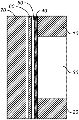
1. A thin-film memory transistor, comprising a source region, a drain region, a channel region, a gate electrode, and a charge-trapping layer provided for charge storage between the channel region and the gate electrode and electrically isolated therefrom, wherein the charge-trapping layer comprises a silicon-rich nitride, with a thickness that is less than 1.0 nm and a trap-site area density of less than 2.7×10¹² electrons per cm2.