| CPC H01L 29/41775 (2013.01) [H01L 21/31116 (2013.01); H01L 29/161 (2013.01); H01L 29/42364 (2013.01); H01L 29/495 (2013.01); H01L 29/6653 (2013.01); H01L 29/66545 (2013.01); H01L 29/66575 (2013.01); H01L 29/7843 (2013.01); H01L 29/165 (2013.01); H01L 29/6656 (2013.01); H01L 29/7848 (2013.01)] | 10 Claims |
|
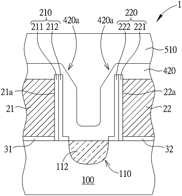
1. A method for fabricating a semiconductor device, comprising:
providing a substrate;
forming a first gate and a second gate on the substrate with a gap between the first and second gates, wherein the first gate has a first sidewall, and the second gate has a second sidewall directly facing the first sidewall, and wherein a first sidewall spacer is disposed on the first sidewall, and a second sidewall spacer is disposed on the second sidewall;
depositing a contact etch stop layer on the first and second gates and on the first and second sidewall spacers;
depositing a protection layer on the contact etch stop layer, wherein the protection layer comprises a silicon dioxide layer;
subjecting the contact etch stop layer to a plasma etching process to trim a corner portion of the contact etch stop layer; and
depositing an inter-layer dielectric layer on the contact etch stop layer and into the gap.
|