| CPC H01L 29/36 (2013.01) [H01L 21/02164 (2013.01); H01L 21/26513 (2013.01); H01L 21/28537 (2013.01); H01L 21/3065 (2013.01); H01L 29/66143 (2013.01); H01L 29/872 (2013.01)] | 19 Claims |
|
1. A method of forming a semiconductor structure, the method comprising:
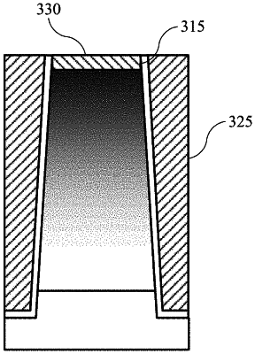
forming a doped silicon layer on a semiconductor substrate, wherein a level of doping is increased at an increasing distance from the semiconductor substrate;
etching the doped silicon layer to define a trench extending to the semiconductor substrate, wherein the doped silicon layer defines a sloping sidewall of the trench, and wherein the trench is characterized by a depth of greater than or about 30 μm;
lining the trench with a first oxide material;
depositing a second oxide material within the trench; and
forming a contact to produce a power device.
|