| CPC H01L 29/0843 (2013.01) [H01L 21/823418 (2013.01); H01L 21/823431 (2013.01); H01L 29/0665 (2013.01); H01L 29/6656 (2013.01); H01L 29/6681 (2013.01)] | 20 Claims |
|
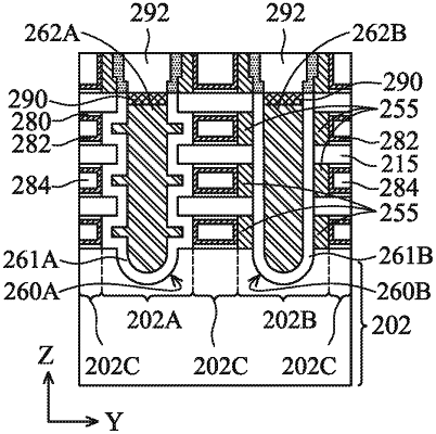
1. A semiconductor device, comprising:
channel layers disposed on a semiconductor substrate;
a gate stack wrapping around each of the channel layers;
a source feature and a drain feature interposed by the gate stack and connecting each of the channel layers; and
inner spacer of a dielectric material disposed between the drain feature and the gate stack, wherein the source feature directly contacts the gate stack, and wherein the drain feature is separated from the gate stack by inner spacers.
|