| CPC H01L 28/75 (2013.01) [H01G 4/008 (2013.01); H01G 4/10 (2013.01); H10B 12/315 (2023.02)] | 17 Claims |
|
1. A semiconductor device comprising:
a substrate; and
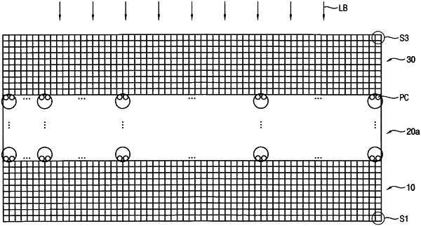
a plurality of memory cell structures arranged on the substrate and electrically connected to surroundings through a contact structure, a support, and a capacitor,
wherein the capacitor comprises
a lower electrode comprising a first metal material and having a crystal size of a few nanometers in such a configuration that the lower electrode is connected with the contact structure and supported by at least the support,
a dielectric layer comprising dielectric material covering the first metal material, the dielectric material comprising merged crystals that each include a plurality of crystals, the merged crystals having a crystal size that is a value of a crystal expansion ratio times the crystal size of the first metal material, wherein the crystal expansion ratio is an integer, and
an upper electrode covering the dielectric layer, the upper electrode comprising a second metal material and having a crystal size smaller than the crystal size of the dielectric material.
|