| CPC H01L 27/156 (2013.01) [H01L 25/0753 (2013.01); H01L 33/483 (2013.01); H01L 33/50 (2013.01); H01L 33/60 (2013.01); H01L 33/62 (2013.01); H01L 33/644 (2013.01); H01L 33/64 (2013.01); H01L 2224/32225 (2013.01); H01L 2224/48091 (2013.01); H01L 2224/48227 (2013.01); H01L 2224/73265 (2013.01); H01L 2924/00014 (2013.01)] | 20 Claims |
|
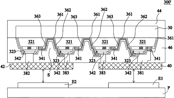
1. An optoelectronic device, comprising:
an epitaxial stack, comprising a first semiconductor layer, an active layer, and a second semiconductor layer;
a trench exposing a portion of the first semiconductor layer;
a first insulating layer formed on a side wall of the trench to electrically insulate from the active layer and the second semiconductor layer;
a first electrode formed on the trench;
a second electrode formed on the second semiconductor layer;
a supporting device covering the epitaxial stack;
an optical layer covering the first electrode and the second electrode, comprising a plurality of openings corresponding to positions of the first electrodes and the second electrodes;
a fifth electrode electrically connected with the first electrode; and
a sixth electrode electrically connected with the second electrode,
wherein the fifth electrode and the sixth electrode each comprises a side comprising a length longer than that of an edge of the epitaxial stack, and the fifth electrode and the sixth electrode each comprises an outer boundary beyond an outer boundary of the epitaxial stack.
|