US 11,705,479 B2
Display apparatus and method of manufacturing the same
Junhee Choi, Seongnam-si (KR); Sungjin Kang, Seoul (KR); Kiho Kong, Suwon-si (KR); Junghun Park, Yongin-si (KR); Jinjoo Park, Yongin-si (KR); Joohun Han, Hwaseong-si (KR); and Kyungwook Hwang, Hwaseong-si (KR)
Assigned to SAMSUNG ELECTRONICS CO., LTD., Suwon-si (KR)
Filed by SAMSUNG ELECTRONICS CO., LTD., Suwon-si (KR)
Filed on Aug. 12, 2021, as Appl. No. 17/400,354.
Application 17/400,354 is a division of application No. 16/589,359, filed on Oct. 1, 2019, granted, now 11,121,171.
Claims priority of application No. 10-2018-0148772 (KR), filed on Nov. 27, 2018.
Prior Publication US 2021/0375983 A1, Dec. 2, 2021
This patent is subject to a terminal disclaimer.
Int. Cl. H01L 27/15 (2006.01); H01L 33/00 (2010.01); H01L 33/14 (2010.01); H01L 33/22 (2010.01); H01L 33/40 (2010.01); H01L 33/42 (2010.01); H01L 33/50 (2010.01); H01L 33/60 (2010.01)
CPC H01L 27/156 (2013.01) [H01L 33/0093 (2020.05); H01L 33/145 (2013.01); H01L 33/22 (2013.01); H01L 33/405 (2013.01); H01L 33/42 (2013.01); H01L 33/504 (2013.01); H01L 33/60 (2013.01); H01L 2933/0016 (2013.01); H01L 2933/0041 (2013.01); H01L 2933/0058 (2013.01); H01L 2933/0091 (2013.01)] 10 Claims
OG exemplary drawing
 
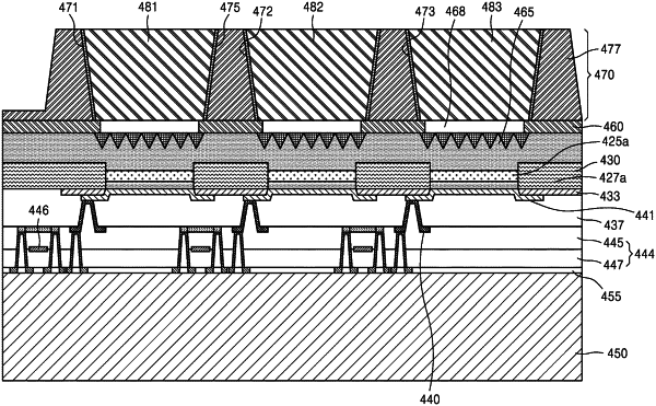
1. A display apparatus comprising:
a support substrate;
a driving layer provided on the support substrate and comprising a driving element;
a light-emitting layer comprising a first semiconductor layer, an active layer, and a second semiconductor layer stacked on the driving layer, the light-emitting layer having an ion implantation region configured to divide light emitted from the active layer into a plurality of subpixels;
a first electrode electrically connected to the first semiconductor layer; and
a second electrode electrically connected to the second semiconductor layer.