| CPC H01L 27/14649 (2013.01) [H01L 27/14629 (2013.01); H01L 27/14636 (2013.01); H01L 27/14683 (2013.01)] | 20 Claims |
|
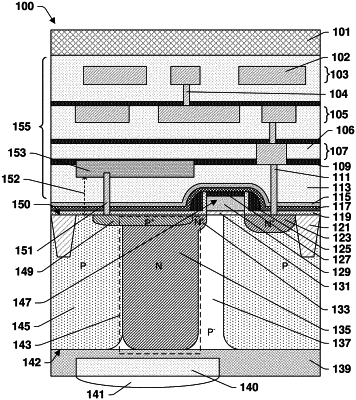
1. An integrated circuit (IC) device, comprising:
a semiconductor substrate;
a photodiode formed within the semiconductor substrate;
an interlevel dielectric layer directly over the photodiode;
a reflector over the interlevel dielectric layer;
a metallization layer over the interlevel dielectric layer; and
an etch stop layer over the interlevel dielectric layer;
wherein a top of the etch stop layer is above a top of the reflector;
a bottom of the etch stop layer is below the top of the reflector; and
the reflector is grounded.
|
|
10. An integrated circuit (IC) device, comprising:
a semiconductor substrate;
a photodiode formed within the semiconductor substrate;
a reflector over the semiconductor substrate; and
a contact plug directly below the reflector;
wherein the reflector is electrically coupled to the semiconductor substrate through the contact plug.
|
|
16. A method of manufacturing an integrated circuit (IC) device, comprising:
forming a photodiode array in a semiconductor substrate;
forming a first dielectric layer over the semiconductor substrate;
forming a hard mask over the first dielectric layer;
using the hard mask to selectively etch a first opening partway through the first dielectric layer;
filing the first opening with a first metal;
planarizing the first metal to form a reflector;
forming a second dielectric layer over the semiconductor substrate
forming a second opening through the second dielectric layer, wherein the second opening lands on the reflector; and
filling the second opening with a second metal to form a metal structure that is electrically coupled to the reflector.
|