| CPC H01L 27/14629 (2013.01) [H01L 27/14607 (2013.01)] | 20 Claims |
|
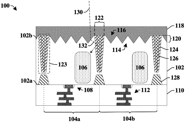
1. An integrated chip, comprising:
a photodetector arranged within a semiconductor substrate;
one or more isolation structures arranged within one or more trenches defined by sidewalls of the semiconductor substrate arranged on opposing sides of the photodetector; and
wherein the one or more trenches extend from a first side of the semiconductor substrate to within the semiconductor substrate, wherein the one or more isolation structures respectively comprise a reflective medium including a metal configured to reflect electromagnetic radiation, and wherein the metal has a topmost surface and a bottommost surface that both extend between outermost sidewalls of the metal, the outermost sidewalls of the metal being directly and laterally between the sidewalls of the semiconductor substrate.
|