| CPC H01L 27/124 (2013.01) | 20 Claims |
|
1. An electronic device, comprising:
a substrate;
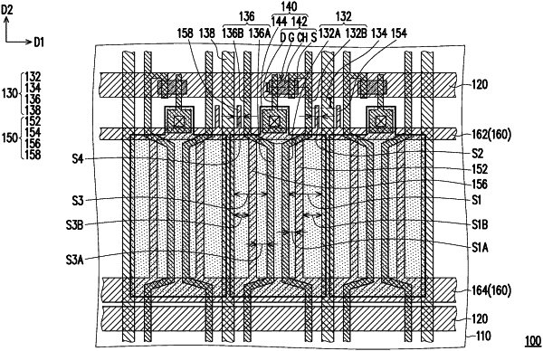
a plurality of transversal signal lines, extending in a first direction, disposed on the substrate;
a first vertical signal line, extending in a second direction, disposed on the substrate, intersected with the transversal signal lines;
a second vertical signal line, disposed on the substrate, intersected with the transversal signal lines, connected to one of the transversal signal lines;
a shielding wire, wherein an orthogonal projection of the shielding wire on the substrate is located between an orthogonal projection of the first vertical signal line on the substrate and an orthogonal projection of the second vertical signal line on the substrate; and
a plurality of pixel structures, wherein one of the pixel structures is surrounded by a corresponding one of the transversal signal lines and the second vertical signal line and comprises an active device, wherein a gate of the active device is electrically connected to the corresponding one of the transversal signal lines, and a source of the active device is electrically connected to the first vertical signal line,
wherein the first vertical signal line comprises a transversal shift section, and one of the pixel structures further comprises a pixel electrode, the pixel electrode is connected to a drain of the active device, and the pixel electrode is overlapped with the transversal shift section and the shielding wire.
|