| CPC H01L 27/1225 (2013.01) [H01L 27/1255 (2013.01); H01L 27/1288 (2013.01); H01L 28/60 (2013.01); H01L 29/41733 (2013.01); H01L 29/45 (2013.01); H01L 29/66969 (2013.01); H01L 29/7869 (2013.01)] | 20 Claims |
|
1. A panel, comprising:
a substrate;
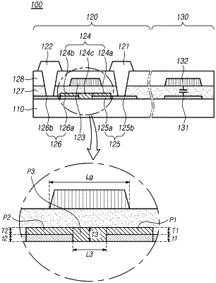
a transistor disposed on the substrate and including:
a source electrode,
a drain electrode,
a gate electrode,
a gate insulation layer,
an active layer,
an auxiliary source electrode configured to electrically connect one end of the active layer to the source electrode with a contact surface between the auxiliary source electrode and the source electrode not overlapped with the active layer in a plan view, and
an auxiliary drain electrode configured to electrically connect another end of the active layer to the drain electrode with a contact surface between the auxiliary drain electrode and the drain electrode not overlapped with the active layer in the plan view; and
a capacitor disposed on the substrate and including a first plate and a second plate,
wherein the first plate of the capacitor includes a same material as the auxiliary source electrode and the auxiliary drain electrode,
wherein at least one of the auxiliary source electrode and the auxiliary drain electrode includes a metal or a conductive oxide including one of Indium Tin Oxide (ITO), Indium Zinc Oxide (IZO), ZnO, SnO2, TiO2, Ga-doped ZnO (GZO), and Al-doped ZnO (AZO),
wherein the first plate of the capacitor is spaced apart from the auxiliary source electrode electrically connecting the active layer to the source electrode and the auxiliary drain electrode electrically connecting the active layer to the drain electrode, and does not overlap any of the source electrode and the drain electrode in the plan view, and
wherein at least one of a part of the auxiliary source electrode and a part of the auxiliary drain electrode overlaps the gate electrode in the plan view.
|