| CPC H01L 27/0886 (2013.01) [H01L 21/823431 (2013.01); H01L 21/823481 (2013.01); H01L 29/42392 (2013.01); H01L 29/785 (2013.01); H01L 29/78696 (2013.01)] | 20 Claims |

|
1. A method for forming a semiconductor device, the method comprising:
receiving a workpiece comprising:
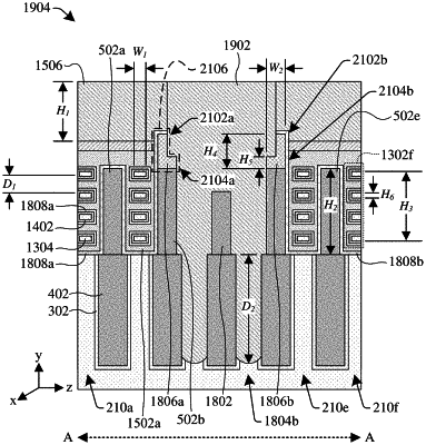
a dielectric fin disposed over a semiconductor substrate and laterally between a first plurality of semiconductor nanostructures and a second plurality of semiconductor nano structures;
a first conductive gate structure disposed over the semiconductor substrate and around the first plurality of semiconductor nanostructures;
a second conductive gate structure disposed over the semiconductor substrate and around the second plurality of semiconductor nanostructures; and
a dielectric fin helmet overlying the dielectric fin, wherein both the dielectric fin helmet and the dielectric fin are disposed laterally between the first conductive gate structure and the second conductive gate structure, and wherein an upper surface of the first conductive gate structure and an upper surface of the second conductive gate structure are both vertically disposed between a first upper surface of the dielectric fin helmet and the semiconductor substrate;
forming a dielectric layer over the dielectric fin, the first plurality of semiconductor nanostructures, the second plurality of semiconductor nanostructures, the first conductive gate structure, the second conductive gate structure, and the dielectric fin helmet;
forming a first opening in the dielectric layer, wherein the first opening at least partially overlies the dielectric fin helmet and the second conductive gate structure; and
removing the second conductive gate structure by performing a first etching process that exposes the second conductive gate structure to a first etchant via the first opening.
|