| CPC H01L 27/088 (2013.01) [H01L 21/76895 (2013.01); H01L 21/823412 (2013.01); H01L 21/823418 (2013.01); H01L 23/485 (2013.01); H01L 21/823475 (2013.01); H01L 27/0207 (2013.01); H01L 27/092 (2013.01)] | 20 Claims |

|
1. A method for forming a semiconductor structure, the method comprising:
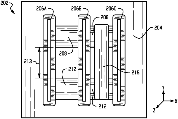
forming a first active semiconductor region disposed in a first vertical level of the semiconductor structure in a substrate;
forming a second active semiconductor region disposed in the first vertical level in the substrate, wherein the second active semiconductor region being separated from the first active semiconductor region in a first direction;
forming a first conductive structure disposed in a second vertical level that is adjacent to the first vertical level, wherein the second vertical level is a single layer of the semiconductor structure, the first conductive structure extending along the first direction as a single piece formed on a first source/drain region of a first transistor and a second source/drain region of a second transistor and electrically coupling the first source/drain region to the second source/drain region;
forming the first source/drain region in the first active semiconductor region on a side of a gate over the substrate; and
forming the second source/drain region in the second active semiconductor region on the side of the gate.
|