| CPC H01L 27/0688 (2013.01) [H01L 21/4857 (2013.01); H01L 23/3171 (2013.01); H01L 23/481 (2013.01); H01L 23/5226 (2013.01); H01L 23/562 (2013.01); H01L 24/03 (2013.01); H01L 24/06 (2013.01); H01L 24/89 (2013.01); H01L 2224/02372 (2013.01); H01L 2224/03916 (2013.01); H01L 2224/80001 (2013.01)] | 20 Claims |
|
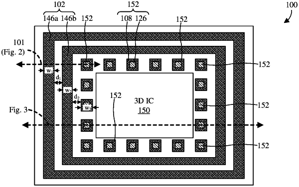
1. A three-dimensional (3D) integrated circuit (IC) comprising:
a first IC die comprising a first semiconductor device disposed in a first semiconductor substrate and a first interconnect structure over the first semiconductor substrate;
a second IC die bonded to the first IC die, wherein the second IC die comprises a second semiconductor device disposed in a second semiconductor substrate and a second interconnect structure over the second semiconductor substrate; and
a plurality of electrical coupling structures arranged at a peripheral region of the first semiconductor device and the second semiconductor device, wherein the plurality of electrical coupling structures respectively comprises a through silicon via (TSV) disposed in the second semiconductor substrate and electrically coupled to the first semiconductor device through a stack of wiring layers and inter-wire vias.
|