| CPC H01L 25/0753 (2013.01) [H01L 25/075 (2013.01); H01L 27/153 (2013.01); H01L 27/156 (2013.01)] | 3 Claims |
|
1. A manufacturing method of a micro LED display device, comprising:
providing a display substrate comprising a plurality of conductive pad pairs arranged in an array;
providing a carrier configured with a plurality of micro light-emitting elements;
providing a transfer element; and
transferring the micro light-emitting elements from the carrier to the display substrate through the transfer element, and electrically bonding the micro light-emitting elements to the conductive pad pairs,
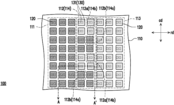
wherein in an nth transferring step, the transfer element is aligned with the carrier, and the transfer element generates a first pattern transfer area to transfer a part of the micro light-emitting elements in a region of the carrier to the display substrate according to the first pattern transfer area, and retain the other micro light-emitting elements in the region, and define a plurality of vacancy positions in a splicing area of the display substrate within a range corresponding to the region,
in another transferring step, the transfer element is aligned with the carrier, and the transfer element generates a second pattern transfer area to transfer the micro light-emitting elements to the display substrate according to the second pattern transfer area to fill the vacancy positions defined in the nth of transfer,
wherein n is a positive integer greater than or equal to 1,
wherein the display substrate has a first arranging area, a first sub-splicing area connected to the first arranging area, a second arranging area and a second sub-splicing area connected to the second arranging area, and the first sub-splicing area and the second sub-splicing area are overlapped with each other to form the splicing area located between the first arranging area and the second arranging area,
wherein the first pattern transfer area is corresponding to the first arranging area and the splicing area, and the second transfer area is corresponding to the second arranging area and the splicing area.
|