| CPC H01L 25/0657 (2013.01) [H01L 25/50 (2013.01); H01L 2224/32225 (2013.01); H01L 2924/15311 (2013.01); H01L 2924/181 (2013.01)] | 22 Claims |
|
1. An apparatus comprising:
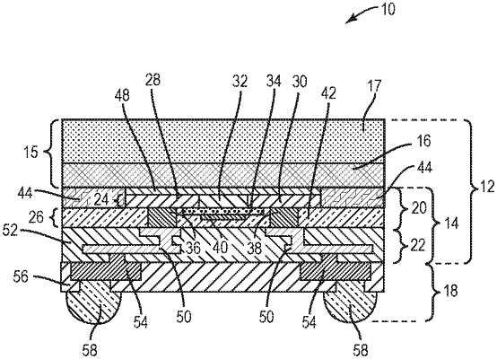
a transfer device die comprising a device region and a transfer substrate, wherein:
the device region includes a front-end-of-line (FEOL) portion and a back-end-of-line (BEOL) portion underneath the FEOL portion, wherein the FEOL portion comprises isolation sections and an active layer, which is surrounded by the isolation sections and does not extend vertically beyond the isolation sections;
a top surface of the device region is planarized; and
the transfer substrate comprising a porous silicon (PSi) region resides over the top surface of the device region, wherein the PSi region has a porosity between 1% and 80%; and
a multilayer redistribution structure formed underneath the BEOL portion of the transfer device die, wherein the multilayer redistribution structure comprises a plurality of bump structures, which are on a bottom surface of the multilayer redistribution structure and electrically coupled to the FEOL portion of the transfer device die.
|