| CPC H01L 24/33 (2013.01) [H01L 21/30625 (2013.01); H01L 21/31053 (2013.01); H01L 21/561 (2013.01); H01L 21/76898 (2013.01); H01L 23/3128 (2013.01); H01L 23/3135 (2013.01); H01L 23/481 (2013.01); H01L 24/05 (2013.01); H01L 24/32 (2013.01); H01L 25/50 (2013.01); H01L 24/13 (2013.01); H01L 2224/02331 (2013.01); H01L 2224/02372 (2013.01); H01L 2224/0401 (2013.01); H01L 2224/05569 (2013.01); H01L 2224/13024 (2013.01); H01L 2224/32057 (2013.01); H01L 2224/32221 (2013.01); H01L 2224/33051 (2013.01)] | 20 Claims |
|
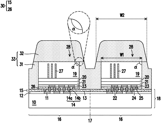
1. A package structure, comprising:
a first die;
a first dielectric layer, covering a bottom surface of the first die, wherein the first dielectric layer comprises a first edge portion and a first center portion in contact with the bottom surface of the first die;
a second dielectric layer, disposed on the first dielectric layer and laterally surrounding the first die, wherein the second dielectric layer comprises a second edge portion and a second center portion, the second edge portion is located on the first edge portion, and the second edge portion is thinner than the second center portion; and
a carrier, bonded to the first dielectric layer through a bonding film.
|