| CPC H01L 24/14 (2013.01) [H01L 23/31 (2013.01); H01L 23/53238 (2013.01); H01L 23/562 (2013.01)] | 20 Claims |
|
1. A semiconductor package, comprising:
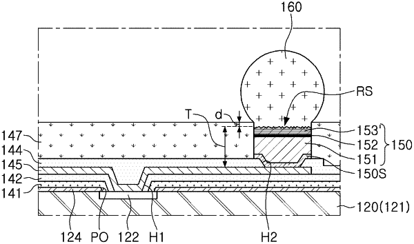
a semiconductor chip including an active surface and a contact pad on the active surface;
a first insulating layer on the active surface, the first insulating layer including a first opening that exposes the contact pad;
a redistribution layer connected to the contact pad, the redistribution layer extending to an upper surface of the first insulating layer;
a second insulating layer on the first insulating layer, the second insulating layer including a second opening that exposes a contact region of the redistribution layer;
a conductive post on the contact region, the conductive post including an intermetallic compound (IMC) layer, the IMC layer being spaced apart from the second insulating layer, an upper surface of the IMC layer being higher than an upper surface of the second insulating layer such that the upper surface of the IMC layer is farther from the active surface of the semiconductor chip compared to the upper surface of the second insulating layer;
an encapsulation layer on the second insulating layer, the encapsulation layer surrounding the conductive post, an upper surface of the encapsulation layer being higher than the upper surface of the IMC layer; and
a conductive bump on an upper surface of the conductive post, the conductive bump contacting the IMC layer, and an interface between the IMC layer and the conductive bump having an uneven surface.
|