| CPC H01L 23/66 (2013.01) [H01L 23/3672 (2013.01); H01L 23/3733 (2013.01); H01L 23/49822 (2013.01); H01L 23/49838 (2013.01); H01L 24/16 (2013.01); H01Q 1/02 (2013.01); H01Q 1/2283 (2013.01); H01L 2223/6677 (2013.01); H01L 2224/16227 (2013.01); H01L 2924/0103 (2013.01); H01L 2924/014 (2013.01); H01L 2924/0105 (2013.01); H01L 2924/01029 (2013.01); H01L 2924/01047 (2013.01); H01L 2924/01049 (2013.01); H01L 2924/01051 (2013.01); H01L 2924/01083 (2013.01); H01L 2924/18161 (2013.01)] | 12 Claims |
|
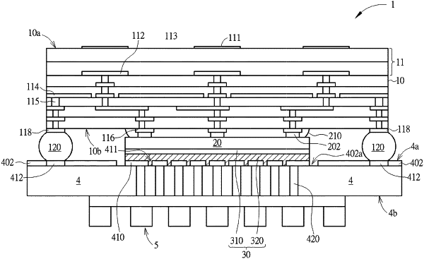
1. A printed circuit board assembly, comprising:
a print circuit board (PCB) having an upper surface directly facing the lower surface of the base, wherein the PCB comprises an array of conductive thermal pads on the upper surface of the PCB, a plurality of thermal vias within the PCB under the array of conductive thermal pads, a heat spreading structure mounted onto a lower surface of the PCB, wherein the heat spreading structure is in thermal contact with the plurality of thermal vias; and
a semiconductor package mounted on the array of conductive thermal pads, the semiconductor package comprising:
a base comprising an upper surface and a lower surface that is opposite to the upper surface;
a radio-frequency (RF) module embedded near the upper surface of the base;
an integrated circuit (IC) die mounted on the lower surface of the base in a flip-chip manner so that a backside of the IC die is available for heat dissipation;
a plurality of conductive structures disposed on the lower surface of the base and arranged around the IC die; and
a metal thermal interface layer comprising a backside metal layer that is in contact with the backside of the IC die, and a solder paste conformally printed on the backside metal layer, wherein the solder paste is in direct contact with the array of conductive thermal pads, wherein the array of conductive thermal pads comprises slits between the thermal pads and the slits are filled with the solder paste.
|