| CPC H01L 23/66 (2013.01) [H01L 21/4853 (2013.01); H01L 21/4857 (2013.01); H01L 23/3128 (2013.01); H01L 23/49822 (2013.01); H01L 23/49833 (2013.01); H01L 23/49838 (2013.01); H01L 24/16 (2013.01); H01Q 1/2283 (2013.01); H01L 2223/6677 (2013.01); H01L 2224/16227 (2013.01); H01L 2924/1421 (2013.01); H01Q 1/243 (2013.01)] | 12 Claims |
|
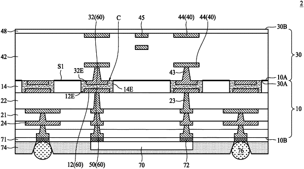
1. An electronic device package, comprising:
a first substrate;
a second substrate disposed over the first substrate;
an encapsulant disposed between the first substrate and the second substrate; and
a conductive element encapsulated by the encapsulant and configured to electrically connect the first substrate to the second substrate,
wherein the encapsulant has a bottom surface, a first upper surface opposite to the bottom surface, and an indented portion between the first upper surface and the bottom surface, and the indented portion is spaced apart from the bottom surface, and
wherein the indented portion of the encapsulant further has a second upper surface and a lateral surface extending between the first upper surface and the second upper surface, and the lateral surface is spaced apart from the conductive element.
|