| CPC H01L 23/66 (2013.01) [H01L 21/6835 (2013.01); H01L 23/3121 (2013.01); H01L 23/552 (2013.01); H01L 24/02 (2013.01); H01L 24/13 (2013.01); H01L 24/19 (2013.01); H01L 24/24 (2013.01); H01L 24/25 (2013.01); H01L 24/32 (2013.01); H01L 25/0655 (2013.01); H01Q 9/045 (2013.01); H01Q 21/0087 (2013.01); H01Q 21/065 (2013.01); H01L 21/568 (2013.01); H01L 21/6836 (2013.01); H01L 23/3128 (2013.01); H01L 23/5389 (2013.01); H01L 2221/68331 (2013.01); H01L 2221/68359 (2013.01); H01L 2221/68372 (2013.01); H01L 2223/6644 (2013.01); H01L 2223/6677 (2013.01); H01L 2224/02331 (2013.01); H01L 2224/02371 (2013.01); H01L 2224/02379 (2013.01); H01L 2224/02381 (2013.01); H01L 2224/04105 (2013.01); H01L 2224/12105 (2013.01); H01L 2224/13024 (2013.01); H01L 2224/24265 (2013.01); H01L 2224/25171 (2013.01); H01L 2224/32225 (2013.01); H01L 2224/73267 (2013.01); H01L 2224/92244 (2013.01); H01L 2224/97 (2013.01); H01L 2924/19041 (2013.01); H01L 2924/19042 (2013.01); H01L 2924/19043 (2013.01); H01L 2924/19104 (2013.01); H01L 2924/3025 (2013.01); H01Q 1/2283 (2013.01); H01Q 21/0075 (2013.01); H01Q 21/22 (2013.01)] | 20 Claims |
|
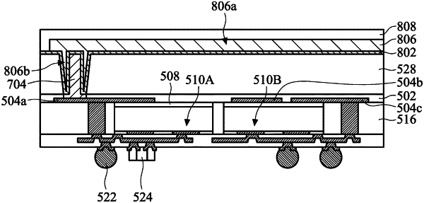
1. A chip package, comprising:
a semiconductor die having a conductive element;
an antenna element over the semiconductor die;
a first conductive feature electrically connecting the conductive element of the semiconductor die and the antenna element;
a protective layer surrounding the first conductive feature; and
a second conductive feature over the first conductive feature, wherein a portion of the second conductive feature is between the first conductive feature and the protective layer, and the first conductive feature is physically separated from the protective layer by the second conductive feature.
|