| CPC H01L 23/66 (2013.01) [H01L 21/565 (2013.01); H01L 23/3114 (2013.01); H01L 23/5226 (2013.01); H01L 2223/6677 (2013.01)] | 20 Claims |
|
1. A semiconductor device, comprising:
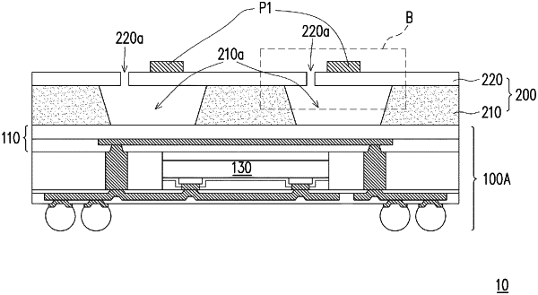
a chip package;
a dielectric structure disposed on the chip package, the dielectric structure comprising a first layer, a second layer disposed between the chip package and the first layer and comprising a cavity, and a vent in communication with the cavity, wherein the first layer covers the cavity, wherein the vent is an air vent; and
a first antenna pattern disposed on the dielectric structure, wherein the chip package is electrically coupled to the first antenna pattern, and the cavity of the dielectric structure is disposed between the chip package and the first antenna pattern.
|