| CPC H01L 23/585 (2013.01) [H01L 23/16 (2013.01); H01L 23/3121 (2013.01); H01L 24/13 (2013.01); H01L 24/32 (2013.01); H01L 24/73 (2013.01); H01L 2224/73204 (2013.01)] | 20 Claims |
|
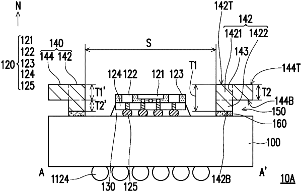
1. A semiconductor package, comprising:
a substrate;
a semiconductor device disposed on the substrate; and
a ring structure disposed on the substrate and surrounds the semiconductor device, the ring structure comprising:
a first portion bonded to the substrate; and
a second portion connecting to the first portion, wherein a cavity is between the second portion and the substrate, and the cavity is spaced apart from a space encircled by the first portion.
|