| CPC H01L 23/5226 (2013.01) [H01L 21/76843 (2013.01); H01L 21/76879 (2013.01); H01L 21/76883 (2013.01); H01L 21/76888 (2013.01); H01L 23/481 (2013.01); H01L 23/528 (2013.01); H01L 23/53228 (2013.01); H01L 23/53257 (2013.01); H01L 23/53266 (2013.01); H01L 29/78 (2013.01)] | 20 Claims |
|
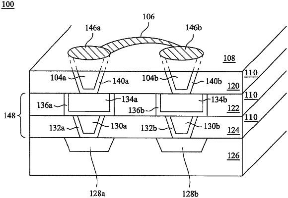
1. A semiconductor device, comprising:
a plurality of vertical conductive structures, wherein each of the plurality of vertical conductive structures extends through an isolation layer; and
an insulated extension disposed horizontally between a first vertical conductive structure and a second vertical conductive structure of the plurality of vertical conductive structures, wherein the insulated extension comprises an insulation depth extending into a portion of the isolation layer between the first and second vertical conductive structure, wherein the insulated extension is separated from both the first and second vertical conductive structures.
|