| CPC H01L 23/49838 (2013.01) [H01L 21/481 (2013.01); H01L 21/486 (2013.01); H01L 21/4853 (2013.01); H01L 23/49827 (2013.01); H01L 23/49894 (2013.01); H01L 23/5384 (2013.01); H01L 25/18 (2013.01)] | 20 Claims |
|
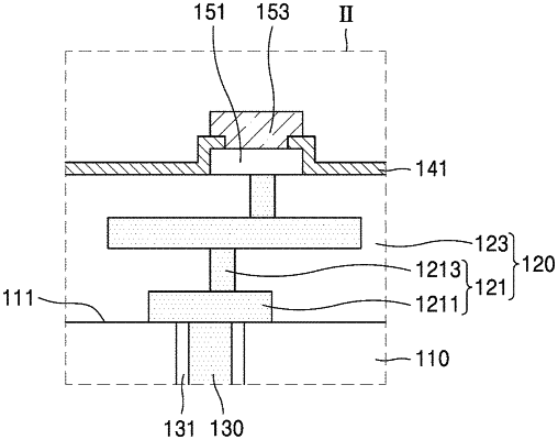
1. A method of manufacturing an interposer, the method comprising:
preparing a base substrate comprising a through electrode;
forming, on a top surface of the base substrate, an interconnection structure comprising a metal interconnection pattern;
forming, on the interconnection structure, a connection pad electrically connected to the metal interconnection pattern of the interconnection structure;
forming, on the interconnection structure, an upper passivation layer having compressive stress, a bottom region of the upper passivation layer including a first silicon oxide layer, and a bottom surface of the upper passivation layer being coplanar with a bottom surface of the connection pad;
forming, on a bottom surface of the base substrate, a lower passivation layer having compressive stress that is less than the compressive stress of the upper passivation layer; and
forming, on the lower passivation layer, a lower conductive layer electrically connected to the through electrode.
|