| CPC H01L 23/49838 (2013.01) [H01L 23/66 (2013.01); H01L 2223/6616 (2013.01); H01L 2223/6638 (2013.01)] | 20 Claims |
|
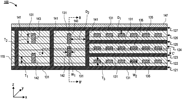
1. An electronic package, comprising:
a package substrate,
wherein the package substrate comprises alternating metal layers and dielectric layers;
a first trace embedded in the package substrate,
wherein the first trace has a first thickness that extends from a bottom of a first metal layer to a top of a second metal layer,
the second metal layer above the first metal layer,
and wherein the first trace has a same width throughout the first thickness;
a first ground plane laterally adjacent to a first side of the first trace;
and a second ground plane laterally adjacent to a second side of the first trace,
wherein the first ground plane is electrically coupled to the second ground plane by lateral ground planes,
wherein the first ground plane, the second ground plane, and the lateral ground planes surround the first trace,
and wherein the first thickness extends from the first metal layer to a third metal layer,
wherein the second metal layer is between the first metal layer and the third metal layer.
|