| CPC H01L 23/49827 (2013.01) [H01L 21/486 (2013.01); H01L 23/49894 (2013.01)] | 24 Claims |
|
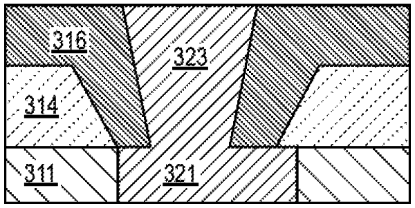
1. An apparatus, comprising:
a via pad at least partially in a core layer;
a first dielectric layer having a first dielectric material above the via pad and the core layer, wherein the first dielectric layer has a first through hole that is through the first dielectric layer to reach the via pad;
a second dielectric layer having a second dielectric material at least partially filling the first through hole, wherein the second dielectric layer has a second through hole that is through the second dielectric layer to reach the via pad, and wherein the second dielectric layer has an uppermost surface; and
a via within the second through hole of the second dielectric layer, surrounded by the second dielectric material, and in contact with the via pad, wherein the via has an uppermost surface at a same level as the uppermost surface of the second dielectric layer.
|