| CPC H01L 23/49527 (2013.01) [H01L 21/4825 (2013.01); H01L 23/3157 (2013.01); H01L 23/49524 (2013.01); H01L 23/49537 (2013.01); H01L 23/49582 (2013.01)] | 17 Claims |
|
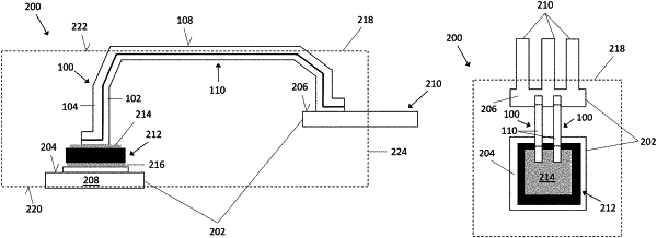
1. A semiconductor package assembly, comprising:
a carrier comprising a die attach surface and a contact pad separated from the die attach surface;
a semiconductor die mounted on the die attach surface, the semiconductor die comprising a front side metallization that faces away from the die attach surface;
an interconnect ribbon attached to the semiconductor die and the contact pad such that the interconnect ribbon electrically connects the front side metallization to the contact pad; and
an electrically insulating encapsulant body that encapsulates the semiconductor die and at least part of the interconnect ribbon,
wherein the interconnect ribbon comprises a layer stack of a first metal layer and a second layer formed on top of the first metal layer,
wherein the first metal layer comprises a different metal as the second metal layer,
wherein the first metal layer faces the front side metallization, and
wherein an upper surface of the ribbon is exposed at an upper surface of the encapsulant body.
|