| CPC H01L 23/481 (2013.01) [H01L 21/4814 (2013.01)] | 20 Claims |
|
1. A method of manufacturing a semiconductor device, the method comprising:
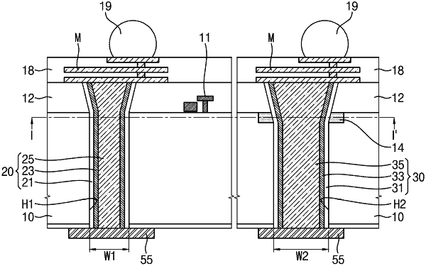
forming an etch stop layer in an upper portion of a substrate;
forming a FEOL structure including an interlayer insulating layer on the substrate and the etch stop layer;
forming a mask pattern including a first open region and a second open region wider than the first open region on the interlayer insulating layer, the second open region vertically overlapping the etch stop layer;
forming a first preliminary through hole and a second preliminary through hole by using the mask pattern as an etch mask, the second preliminary through hole exposing the etch stop layer, the first preliminary through hole is deeper than the second preliminary through hole;
forming a first through hole and a second through hole by extending the first preliminary through hole and the second preliminary through hole in a downward direction using the mask pattern as an etch mask; and
forming a first TSV in the first through hole and a second TSV in the second through hole.
|