| CPC H01L 23/481 (2013.01) [H01L 21/76898 (2013.01); H01L 23/5226 (2013.01)] | 20 Claims |
|
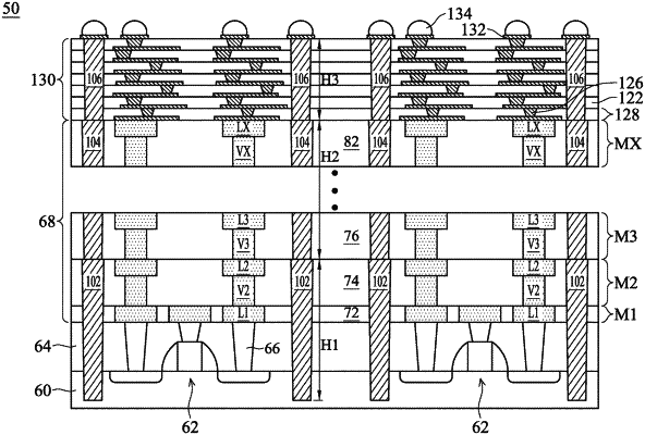
1. A semiconductor structure, comprising:
a semiconductor substrate, the semiconductor substrate having a first side and a second side opposite the first side;
an active device on the first side of the semiconductor substrate;
an interconnect structure on the semiconductor structure, the interconnect structure being over the active device, the interconnect structure comprising a first metallization layer, a second metallization layer over the first metallization layer, a third metallization layer over the second metallization layer, and a fourth metallization layer over the third metallization layer;
a first through via extending through the semiconductor substrate, the first through via extending through the first metallization layer and the second metallization layer; and
a second through via in the interconnect structure, the second through via extending through the third metallization layer and the fourth metallization layer, a bottom surface of the second through via contacting a top surface of the first through via.
|