| CPC H01L 23/3737 (2013.01) [H01L 21/4882 (2013.01); H01L 23/04 (2013.01); H01L 23/3128 (2013.01); H01L 23/4006 (2013.01); H01L 2023/4087 (2013.01)] | 20 Claims |
|
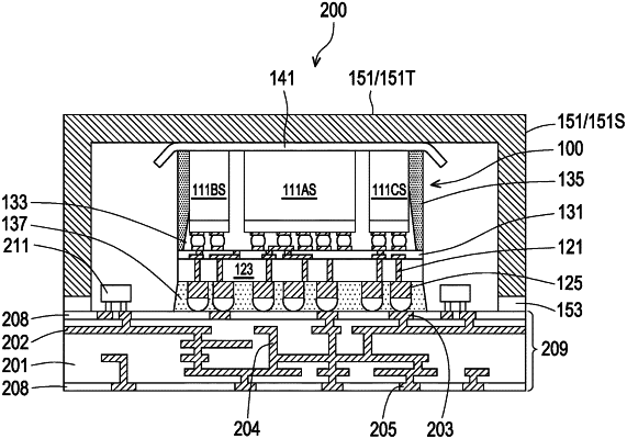
1. A method of forming a semiconductor structure, the method comprising:
attaching a semiconductor device to a first surface of a substrate;
placing a thermal interface material (TIM) film over a first side of the semiconductor device distal from the substrate, wherein the TIM film is pre-formed before the placing, wherein after the placing, a peripheral portion of the TIM film extends laterally beyond sidewalls of the semiconductor device, wherein the peripheral portion of the TIM film extends closer to the substrate than a center portion of the TIM film disposed over a center of the first side of the semiconductor device, wherein the peripheral portion of the TIM film and the center portion of the TIM film have a same thickness; and
attaching a lid to the first surface of the substrate to form an enclosed space between the lid and the substrate, wherein after attaching the lid, the semiconductor device and the TIM film are disposed in the enclosed space, wherein a first side of the TIM film distal from the substrate contacts the lid.
|